How PCB Mismatch Affects Common-N DCR Current Sensing in Multi-phase Applications
Abstract
It has been many years since GPU power solutions (OVR3i+ / OVR4i+) adopt common-N structure for DCR current sensing in multi-phase applications. There are two common-N type multi-phase controllers for graphic core power application in Richtek, the 3 phases controller RT8843A for OVR3i+ solution and the 8 phases controller RT8848A for OVR4i+ solution respectively. The common-N structure has benefit of pin-saving in a limited package size as compared to differential structure of DCR current sensing. However, this structure has an intrinsic drawback of current unbalance issue as PCB layout is not symmetric especially in high phase count applications. High phase count is a trend in computing graphic cards or data mining machines. The layout can’t always be symmetric in a limited board size and even the priority of high speed signal routing for GPU/DDR is much higher than power routing. Therefore, the effect of RPCB non-symmetric on current sensing is a crucial topic in multi-phase applications. Some advanced controller, such as RT8848A, has function of current balance gain adjustment according to each phase by I2C communication is necessary for improving the current balance performance. In this application note, the analysis of common-N structure with different connection types are discussed. Simulation and experiments with RT8848A or RT8843A are also performed to verify the theory. In a result, user can understand the RPCB mismatch effect on different types of common-N DCR current sensing network and choose a suitable method to implement in their application.
1.
Introduction
to DCR Current Sensing Network
The DCR current sensing network has been a popular method for inductor current sensing due to the advantages of power lossless and ease of design. In Figure 1, a standard DCR current sensing circuit is presented. A pair of Rx and Cx is in parallel with inductor L. The inductor model has equivalent inductance in series with a DCR resistor. The voltage signal across Cx can be derived in equation (1). It can be noticed that as the time constant of L and DCR matches Rx and Cx (as shown in equation (2)), then the VCX is equal to the inductor current multiplies DCR value. Both DC and AC signal of inductor current (IL) can be achieved through the voltage of VCX.
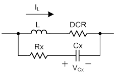
Figure 1. DCR Current Sensing Topology
Assume in s-domain, the VCX voltage can be derived via KCL/KVL rules.

when

By substituting equation (2) into equation (1), the VCX voltage can be represented as following equation.

From above derivation, the inductor current can be achieved via properly designing the parameters of DCR current sensing circuit. In high power applications, such as GPU core power or CPU core power, the high phase number is necessary to achieve enough current capability within a limited inductor size and power stages (MOSFET).
There are two different structures for DCR current sensing in multi-phase applications.
The first one is differential current sense topology as shown inFigure 2. The inductor current is sensed as the voltage across the DCR current sense capacitor. Each phase has individual positive and negative sensing pins to be connected to positive terminal and negative terminal of Cx. Therefore, the voltage across Cx can be well monitored and applied to current balance control and per-phase over-current protection. However, as the phase number increases, the necessary pin number will also increase. This structure has benefit of high accuracy of current sensing, but the high pin count is a trade-off.
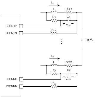
Figure 2. Differential Current Sense Topology
On the other hand, for the second structure which is called as common-N current sense topology is shown in Figure 3. The inductor current signal can be achieved from the voltage sensing across the DCR current sensing capacitor (Cx). Different from differential type, there is only one negative pin (CSN pin) as the reference for each phase’s inductor current signal. The negative points of each phase’s Cx are connected together to the CSN pin as a common-N reference. This structure has benefit of pin-saving, but the current signal has some distortion which can result in current unbalance issues and false triggering over-current protection. In the next section, the analysis of different types of common-N structure will be addressed.
Figure 3. Common-N Current Sense Topology
2.
Analysis
of Different Types of Common-N Structure
There are four types of common-N structure for DCR current sensing in multi-phase applications : Type1, Type2, Type3 and Remoting methods. In this section, the analysis of these structures will be addressed, including the simulation waveforms and RPCB effect derivation on DCR current sensing signal.
2.1 The Type1 Common-N Structure
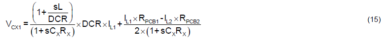
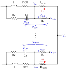
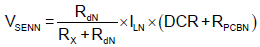
The first type of DCR current sensing connection for common-N structure is shown in Figure 4. For simplification, a two phases condition is applied to derive the equation for discussing the effect of RPCB on DCR current sensing signal. The RPCB shown on the circuit are the layout impedance from inductor output node to regulating point at GPU side. According to different layout arrangement, the RPCB impedance of each phase may be similar or different. Moreover, the deviation between RPCB may generate an additional offset on current feedback signal (VSEN). In order to prevent large leakage current on common-N layout trace, a small resistor Rn is applied to connect each Cx’s negative terminal together. The VSEN signal can be derived by following steps.
First, the Vo1, Vo2 and Vo,av are derived as :


And the VCX can be derived by following equation in s-domain.

From equation (7), the VCX can be represented as :
Then the voltage signals of VSEN1 and VSEN2 are achieved by adding the voltage across Rn to VCX signal.
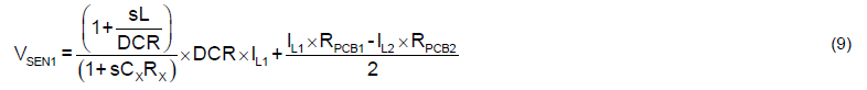
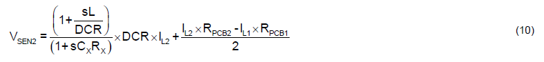
Figure 4. 2 Phases Type1 Common-N DCR Current Sensing Circuit
It can be noticed that the additional offset on VSEN signal makes the controller unable to know the correct current signal. Without knowing the correct current amplitude of each phase, current balance function works abnormally. The current balance can only be achieved if RPCB1 and RPCB2 are the same by layout PCB symmetrically. Practically, it’s very hard to layout PCB symmetrically in high phase application, the current balance performance requires to be improved by adjusting the current balance gain to compensate the additional current offset on VSEN signal. However, if the RPCB deviation is too large as compared to DCR value, the performance of current balance will be limited due to the limited modification range of current balance gain. Moreover, as shown in equation (9) and (10), the current offset items are related to both per-phase inductor current (IL1 and IL2) and RPCB values. Due to the current signal (IL1 and IL2) is the combination of DC current value and AC inductor current ripple, the offset current signal on VSEN has both DC component and AC component. For DC component, it affects the average value of inductor sensing current; and for AC component, it changes the current ripple shape from triangle ripple to an abnormal ripple as shown in Figure 5. In this example, the DCR value is setup as 0.6mΩ, and L/DCR = RxCx for time constant matching. RPCB1 and RPCB2 are setup as 1mΩ and 10mΩ respectively to emulate the PCB non-symmetric issue. The abnormal current ripple may induce controller to false trigger protection functions such as OCP function. For some application as VCORE power, false triggering OCP may result the power rail shutdown and system also shutdown after then. Furthermore, if the current signal is used for output voltage loop control, the stability may become worse.
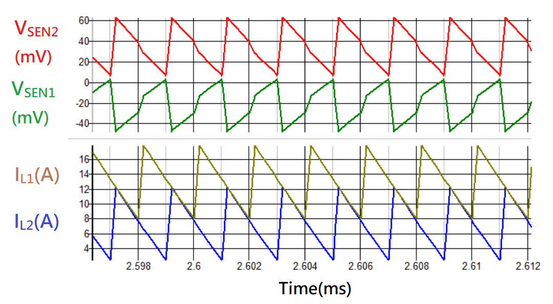
Figure 5. DCR Current Sensing Signal with Type1 Common-N Structure
2.2 The Type2 Common-N Structure
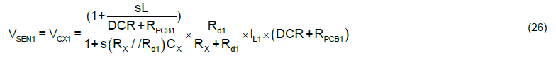
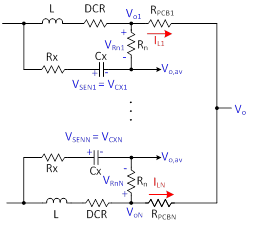
Figure 6 shows the Type2 common-N DCR current sensing circuit. For simplification, a two phases condition is applied to derive the equation for discussing the effect of RPCB on DCR current sensing signal. The RPCB shown on the circuit are the layout impedance from inductor output node to regulating point at GPU side. It can be noticed that the placement of Rn is different from Type1. The Rn is in series with DCR current sensing components (Rx and Cx). The VSEN signal is equal to VCX voltage across DCR current sensing capacitor (Cx). The VSEN signal can be derived by following steps.
First, the Vo1, Vo2 and Vo,av are derived as :


And the VCX1 can be derived by following equation in s-domain.

From equation (14), the VCX1 can be represented as :
Similar to VCX1, the VCX2 can also be derived as below equation :
And the VSEN1 and VSEN2 are equal to VCX1 and VCX2 respectively.
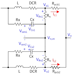
Figure 6. 2 Phases Type2 Common-N DCR Current Sensing Circuit
The VSEN1 and VSEN2 can be achieved from equation (15) and equation (16). When time constant of L/DCR matches RxCx, the DCR current sensing signal equals to the sum of inductor current multiplies DCR of inductor and the additional offset. The additional offset is generated by the deviation of RPCB multiplies inductor current between each phase. The equation of VSEN signal is similar to the equation derived from Type1 structure. The major difference is the AC offset ripple is suppressed by RxCx filter and can be ignored as compared to DC offset. However, the DC offset still affects the current sensing signal. An example of the DCR current sensing signal with type2 common-N structure is shown in Figure 7. It can be observed that each VSEN signal is in shape with its inductor current. In this case, the DCR value is set as 0.6mΩ, and L/DCR = RxCx for time constant matching. RPCB1 and RPCB2 are setup as 1mΩ and 10mΩ respectively to emulate the PCB non-symmetric issue. The VSEN signal of both phase1 and phase2 are not proportional to DCR value due to the additional DC offset on current sensing signal. Therefore, the controller may have a hard time to control the current of each phase to achieve current balance. Moreover, the over-current protection function can’t work correctly as current signal is not accurate. For type 2 connection, the current balance can be improved by adjusting the current balance gain to compensate the Rpcb deviation. However, there is a bottleneck for this method because most of controller has limited adjustment range of current balance gain. In section4, the design tips for Rpcb variation and current balance gain will be discussed.
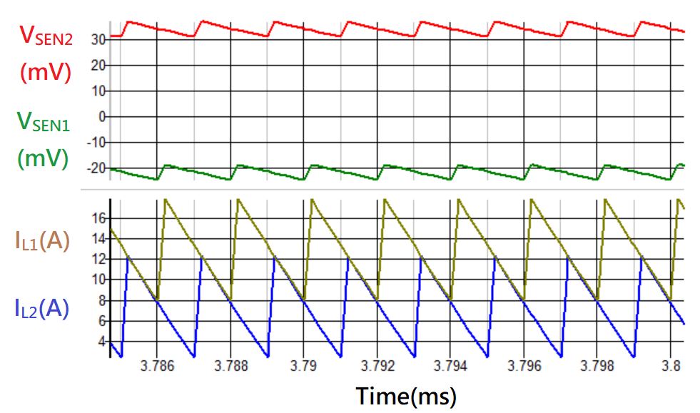
Figure 7. DCR Current Sensing Signal with Type2 Common-N Structure
2.3 The Type3 Common-N Structure
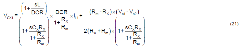
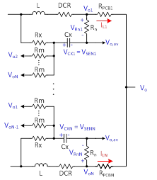
As described in previous sections, both Type1 and Type2 can’t get accurate inductor current signal from VSEN signal. In this section, a method based on Type2 is proposed to eliminate the RPCB effect on VSEN signal. Figure 8 shows a two phases Type3 common-N DCR current sensing circuit. For simplification, a two phases condition is applied to derive the equation for discussing the effect of RPCB on DCR current sensing signal. The RPCB shown on the circuit is the layout impedance from inductor output node to regulating point at GPU side. The resistor Rm is connected from positive terminal of DCR current sensing capacitor (Cx) to the output node of other phase’s inductor. For multiple phases application with Type3, the equivalent circuit is shown in Table 1. In order to simplify the circuit diagram, the wire connections are represented with net names and arrows. It should be noticed that it requires additional Nx(N-1) pcs resistors to connect between each phases’ output when applying Type3 method, where N is the total operating phase number. For example, the total required number of Rm is 2 x (2-1) = 2pcs in a 2 phases application. And for 3 phases application, the total required number of Rm is 3 x (3-1) = 6pcs as shown in Figure 19. The VSEN signal can be derived by following steps.
First, the Vo1, Vo2 and Vo,av are derived as :


And the VCX1 can be derived by following equation in s-domain.

From equation (20), the VCX1 can be represented as :
Similar to VCX1, the VCX2 can also be derived as below equation :
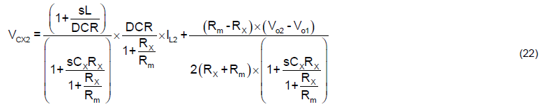
And the VSEN1 and VSEN2 are equal to VCX1 and VCX2 respectively.
For equation (21) and equation (22), if Rm is equal to Rx, the offset items are eliminated, and the equation can be represented as following.
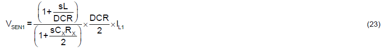
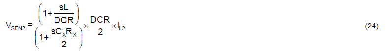
From equation (23) and equation (24), make L/DCR = RxCx/2 for time constant matching, then the current signal can be calculated via inductor current multiplies DCR/2. It should be noticed that the equivalent DCR is divided by 2 due to additional Rm resistor. In a result, the RPCB non-symmetric effect has been cancelled.
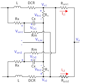
Figure 8. 2 Phases Type3 Common-N DCR Current Sensing Circuit
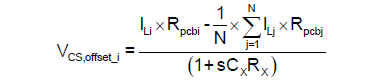
Figure 9 shows an example of the DCR current sensing signal with Type3 common-N structure. In this example, the DCR value is set as 0.6mΩ, and L/DCR = RxCx/2 for time constant matching. RPCB1 and RPCB2 are setup as 1mΩ and 10mΩ respectively to emulate the PCB non-symmetric issue. In this simulation, the current balance function is disabled and the output load current is 20A. The VSEN signal of both phase1 and phase2 are proportional to their inductor current signal with the gain of DCR/2 = 0.3mΩ. Therefore, the PWM controller can get the correct current signal and adjust the PWM pulse width to achieve current balance between each phase. Moreover, over-current protection function also works correctly. The Type3 method is useful in low phase number (< 4phase). If the phase number increases to 8phase, the number of required “Rm” resistor is up to 7x8 = 56pcs. A N phases Type3 structure needs additional (N-1) x N pcs resistor connected to each phase’s inductor output node. Besides, the side effect of Type3 is the DCR reduction, which makes equivalent DCR become DCR/N, where N is the phase number. After DCR reduction, the impact of current sensing comparator offset (Vcs,ofs_comp) becomes crucial as compared to current signal. The current sensing signal including comparator offset can be represented as below :
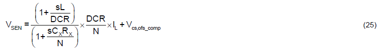
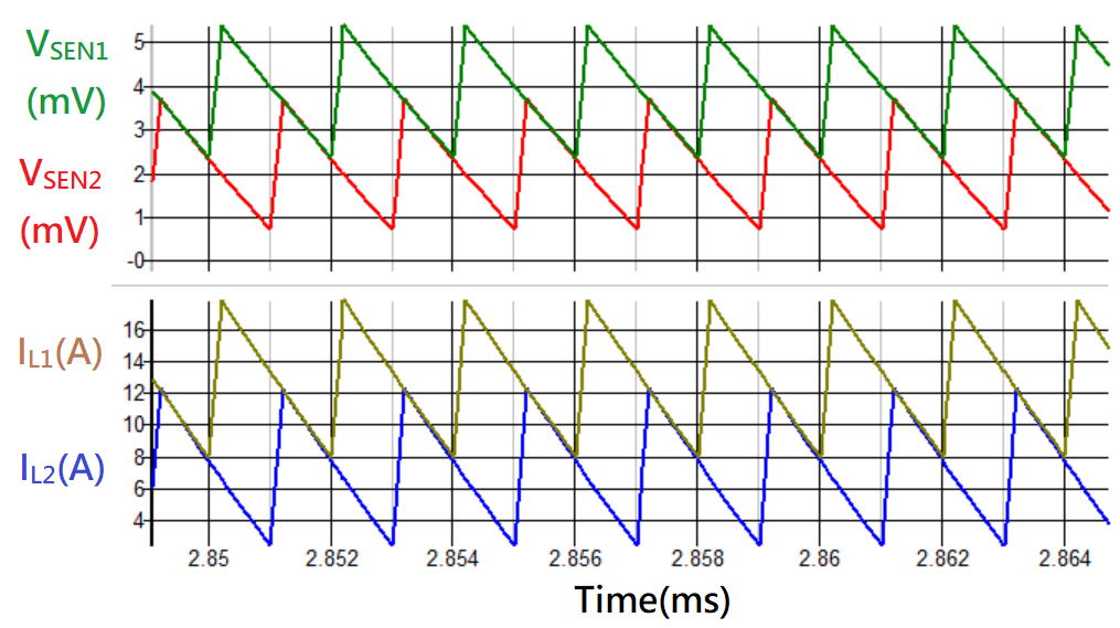
Figure 9. DCR Current Sensing Signal with Type3 Common-N Structure
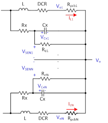
2.4 The Remoting Type Common-N Structure
In this section, an alternative method which can solve the current unbalance issue is proposed. As shown in Figure 10, it’s a N phases common-N DCR current sensing circuit with remoting connection. The main idea of this method is to include each phase’s RPCB value into their own DCR value, where the RPCB is the layout impedance from inductor output node to regulating point at GPU side. The DCR network of Rx and Cx is in parallel with power inductor and RPCB layout impedance. It should be noticed that the negative point of Cx is connected to the remoting sensing point at GPU side. A divider resistor is in parallel with Cx to compensate the deviation of RPCB values between different phases. The VSEN signal can be derived by following steps.
For VSEN1, the equivalent inductor impedance is DCR + RPCB1, and the VCX1 or VSEN1 can be calculated as following equation :
If properly design the parameters to make L/(DCR+RPCB1) = (RX//Rd1)CX, then the VSEN1 is equal to the following equation :

On the other hand, the VSEN signal of the other phases can be derived by the similar method. For instance, the VSEN signal of phase N is shown as below :
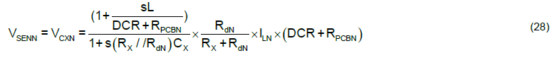
For time constant matching, let L/(DCR+RPCBN) = (RX//RdN)CX, then the VSENN is equal to the following equation :

It should be noticed that the negative terminal of Rd resistor should be routed to the remoting point at GPU side to avoid additional voltage offset on VSEN signal.
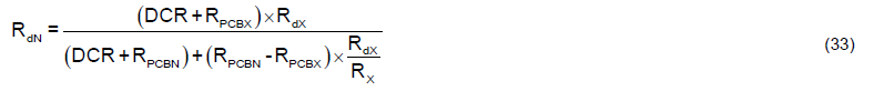
In order to achieve current balance in multi-phase application, the divider resistor Rd should follow the design steps as below.
Step1. Find the minimum value of (DCR + RPCBX) among N phases circuit. Assume RPCBX < RPCB1, …, RPCBN.
Step2. For current balance condition, assume IL1 = IL2 =…= ILN and VSEN1 = VSEN2 =…= VSENN.
Step3. Calculate the Rd value for each phase.
By utilizing the condition in step2, the relation between RdX and the other Rd can be derived as below :
For Rd1,

For RdN,

From equation (30), the Rd1 can be calculated as below :

From equation (31), the RdN can be calculated as below :
In a summary, the RPCB effect on current sensing signal can be solved if considering the RPCB value into the parameters design of DCR current sensing circuit. In Figure 11, the simulation result of a 2 phases DCR current sensing network with remoting type for RPCB cancellation is presented. In this example, the DCR value is set as 0.6mΩ, and (Rx, Cx, Rd1, Rd2) follow equation (26) and equation (28) for time constant matching. RPCB1 and RPCB2 are setup as 1mΩ and 10mΩ respectively to emulate the PCB non-symmetric issue. In this simulation, the current balance function is disabled and the output load current is 20A. The VSEN signal of both phase1 and phase2 are proportional to their inductor current signal with the gain of (DCR + RPCB1) x Rd1 / (Rd1 + Rx) and (DCR + RPCB2) x Rd2 / (Rd2 + Rx) respectively. Therefore, the PWM controller can get the correct current signal and adjust the PWM pulse width to achieve current balance between each phase. Moreover, over-current protection function also works correctly.
In the next section, a practical example of an 8 phase controller which adopts the remoting type common-N circuit to solve the RPCB effect will be performed.
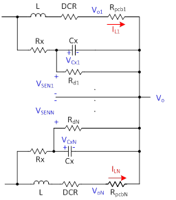
Figure 10. The N Phases Remoting Type Common-N DCR Current Sensing Circuit
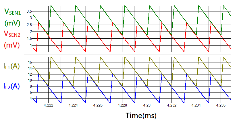
Figure 11. DCR Current Sensing Signal with Remoting Type Common-N Structure
2.5 Summary and Comparison of the Four Types of Common-N DCR Current Sensing Structures
We have introduced four types of common-N DCR current sensing circuit in previous sections. For Type1, there is an offset, which combined both DC and AC terms, on the current sensing signal and the offset influences both current balance and per-phase over-current protection. For Type2, there is a DC offset, which comes from the deviation of RPCB, on the current sensing signal and the offset affects both current balance and per-phase over-current protection. For Type3, the RPCB effect can be cancelled by connecting the positive terminal of CX to each phases’ inductor output nodes. Although the equivalent DCR is reduced by the connected phase number and it needs more resistors in application circuit. This method can effectively solve the current unbalance issue and make per-phase over-current protection function normally. For remoting type, the RPCB is considered with the inductor’s DCR for designing the parameters of DCR current sensing circuit. Therefore, the RPCB effect can be well solved if RPCB values are correct. Table 1 summarized the sensing offset generated from these four types of common-N DCR current sensing circuit.
Table 1. Summary Table of the Four Types of Common-N DCR Current Sensing Structures
|
Type1
|
Type2
|
|
|
|
|
Sensing offset

|
Sensing offset
|
|
Type3
|
Remoting Type
|
|
|
|
|
Sensing offset
1. If Rm = Rx, the PCB effect can be cancelled.
2. Design , then , then 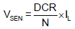
|
Sensing offset
1. If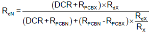 , the PCB effect can be cancelled. , the PCB effect can be cancelled.
2. Design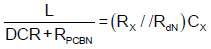
|
3.
Design Consideration for Rn
For common-N DCR current sensing structure, there is only one reference point (VCSN) for current signal detection. As shown in Figure 12, for type 1, 2 and 3, a small resistor Rn is connected between inductor output node and the common-N reference point for each phase. The Rn is applied to limit the leakage current on the trace when there is a voltage drop across inductor output node and common-N point. This voltage drop is generated by the RPCB layout difference between each rail. In order to reduce the leakage current on these traces, we can use a large Rn to limit the current. However, the selection of Rn should also consider the RC time delay on common-N voltage (VCSN). The RC time constant of (Rn, Cn) affects the response time of current feedback signal, if RC time constant is larger than switching period (1/fSW), where fSW is switching frequency of PWM, the current feedback signal will be delayed and the loop response becomes slower. Therefore, the RC time constant should be smaller than switching period to guarantee the transient performance. Generally, the minimum value of Cn is suggested to be larger than 10nF/0603/6.3V for noise filtering on local CSN pin. Then, the selection guide of Rn can follow below criterion :

For example, if Cn is designed with 10nF and fSW = 300kHz, the Rn is recommended to be 50W to minimize the leakage current and also meet design criterion.
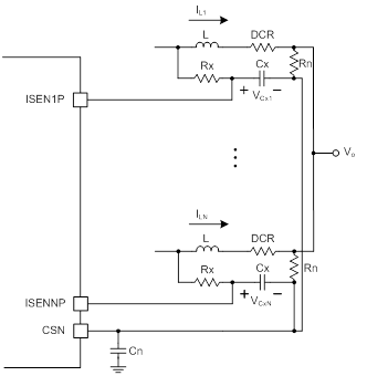
Figure 12. Common-N Current Sense Topology with Rn and Cn
4.
Case Study and Design Tips
In this chapter, some practical application examples with different type of common-N DCR current sensing connection are presented. The simulation results are simulated with the FineSim spice model based on chip-level (Richtek internal design tools.
4.1 Practical Design Example of Type2 Common-N DCR Current Sensing
The Type1 and Type2 DCR current sensing structures are introduced and analyzed in chapter 2. The main difference between these two methods is the the AC offset ripple is suppressed by RxCx filter in Type2 connection. Frankly speaking, Type1 connection is not a recommended method for common-N DCR applications. The additional AC ripple injected into inductor current sensing signal generates the wrong current signal and it is unacceptable for most of IC controllers. Therefore, we will not use Type1 as an example in practical applications. Here we are going to introducing the design limitation according to current balance gain and RPCB values when using the Type2 connection. Then, we will summarize a design rule to make sure the user has enough adjustable range of current balance gain to compensate the RPCB effect. In a result, some practical design examples will be presented.
First, for a given controller which applies common-N DCR current sensing structure, take RT8848A as an example, the RT8848A is an 8 phase multi-phase synchronous Buck controller which is optimized for high performance graphic microprocessor and support Nvidia OVR4i+ specification. A simplified application circuit for describing the DCR current sensing circuit connection is shown in Figure 13. For full application schematic, please refer to RT8848A datasheet [reference 3]. The adjustable range of current balance gain for RT8848A is from 0.68 to 1.24. Therefore, the ratio of maximum gain and minimum gain is calculated by below equation.

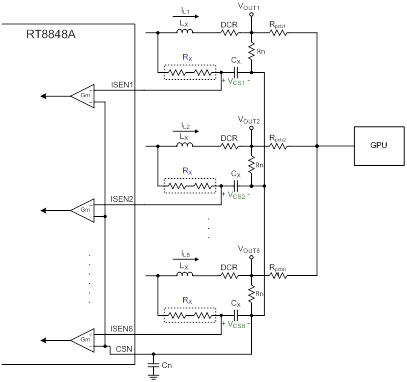
Figure 13. Simplified Application Circuit for RT8848A with Type2 DCR Current Sensing Network
Next, when applying with common-N DCR current sensing network in multi-phase application, the current feedback signal (VCSi) includes both DCR term and Rpcb term as derived in chapter 2. The VCSi for each phase can be represented as below equation.

Where the DCR term is :

And the Rpcb term is :

For current balance adjustment, the maximum current feedback signal (VCS_max) and minimum current feedback signal (VCS_min) should follow the rule as below :

The equation (39) should always be positive. In order to properly compensate the PCB effect with current balance gain, the equation (39) should be considered during PCB layout in practical application. Following are two simulation examples with different PCB layout, the first one has non-symmetric PCB layout and fail to meet equation (39). The second one has relatively symmetric PCB layout and meet equation (39). The simulation performs current balance result from light load to heavy load with 8 phase configuration. As shown in Figure 14, the current balance result of first simulation case is presented. The RPCB values are summarized in Table 2. The current signal ratio between maximum and minimum value can be calculated by substituting the PDN (Power Delivery Network) values to equation (39), and the calculation result is shown below :

From equation (40), it is obvious that the PDN value is over the design criterion. Therefore, the current balance result is worse even with modified current balance gain. The average current of each phase in simulation result at IOUT = 240A are listed in Table 3 and Table 4.
Table 2. PDN Design Value of Non-symmetric PCB Layout
|
Inductor DCR = 0.5mΩ
|
|
RPCB1 = 1.441mΩ
|
RPCB5 = 0.269mW
|
|
RPCB2 = 1.401mΩ
|
RPCB6 = 0.378mΩ
|
|
RPCB3 = 1.399mΩ
|
RPCB7 = 0.426mΩ
|
|
RPCB4 = 1.406mΩ
|
RPCB8 = 0.472mΩ
|
Table 3. Average Current of Each Phase with Default CB Gain (Non-Symmetric PCB Layout)
|
|
PH1
|
PH2
|
PH3
|
PH4
|
PH5
|
PH6
|
PH7
|
PH8
|
Deviation
|
|
IL,avg (A)
|
19.5
|
19.9
|
20
|
19.7
|
44.9
|
40.5
|
38.7
|
37.2
|
±42%
|
Table 4. Average Current of Each Phase with Modified CB Gain (Non-Symmetric PCB Layout)
|
|
PH1
|
PH2
|
PH3
|
PH4
|
PH5
|
PH6
|
PH7
|
PH8
|
Deviation
|
|
IL,avg (A)
|
22.2
|
22.8
|
22.8
|
22.8
|
41.6
|
37.4
|
35.7
|
34.3
|
±33%
|
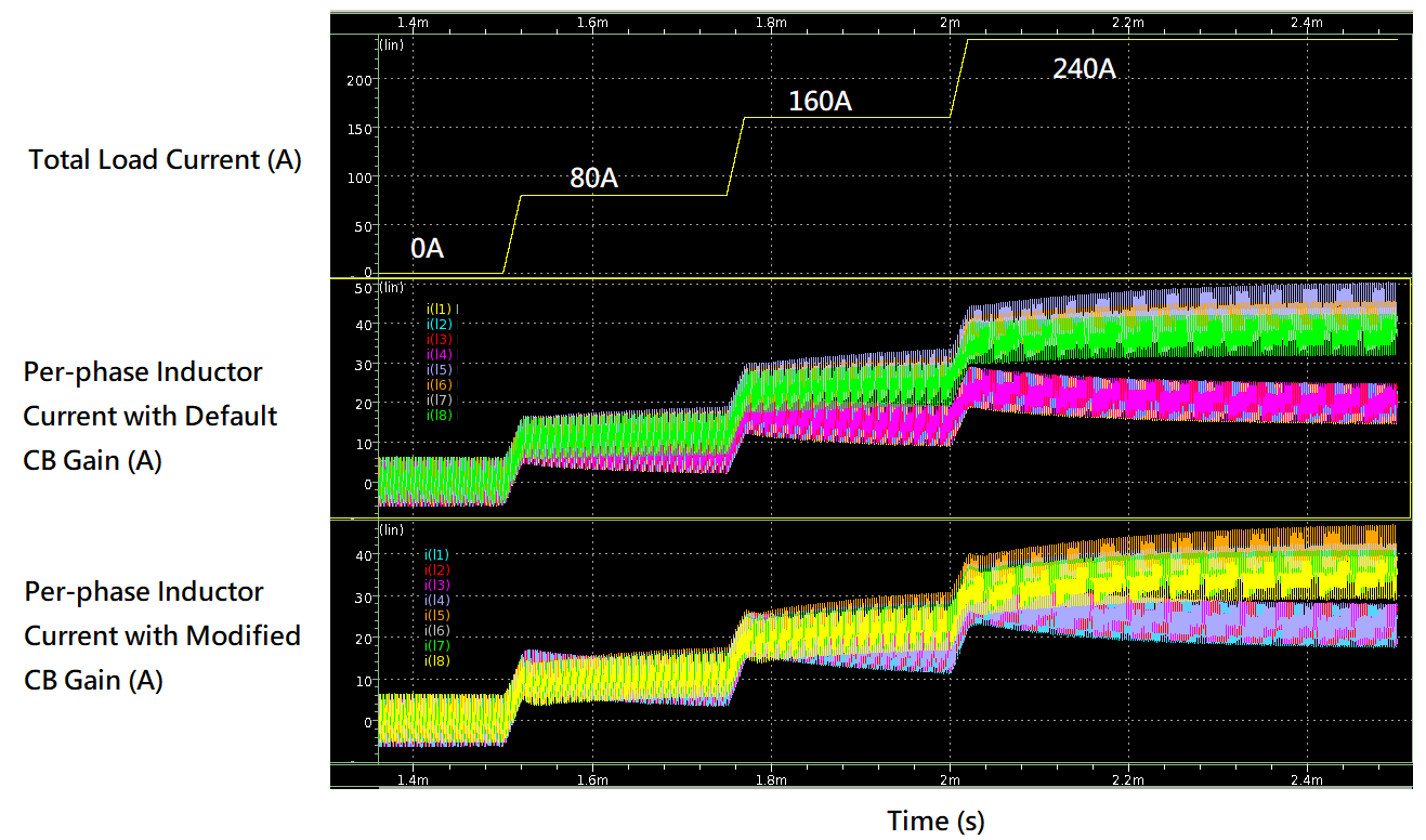
Figure 14. Current Balance Result with Non-symmetric PCB Layout
For the second simulation case as shown in Figure 15, the PDN values are summarized in Table 5. By substituting the PDN values to equation (39), the ratio between VCS_max and VCS_min can be calculated as below :

From equation (41), the result shows the PDN deviation is within the design criterion. Therefore, the current balance result can be improved to an acceptable range by properly setting the current balance gain. If the design range of current balance gain is wider, the current balance performance may be much better. The average current of each phase in simulation result at IOUT = 240A are listed in Table 6 and Table 7.
Table 5. PDN Design Value of Symmetric PCB Layout
|
Inductor DCR = 1mΩ
|
|
RPCB1 = 1.3mΩ
|
RPCB5 = 0.75mΩ
|
|
RPCB2 = 1.25mΩ
|
RPCB6 = 0.8mΩ
|
|
RPCB3 = 1.2mΩ
|
RPCB7 = 0.85mΩ
|
|
RPCB4 = 1.15mΩ
|
RPCB8 = 0.9mΩ
|
Table 6. Average Current of Each Phase with Default CB Gain (Symmetric PCB Layout)
|
|
PH1
|
PH2
|
PH3
|
PH4
|
PH5
|
PH6
|
PH7
|
PH8
|
Deviation
|
|
IL,avg (A)
|
25.9
|
26.5
|
27.1
|
27.6
|
34.7
|
33.8
|
32.8
|
32
|
±15%
|
Table 7. Average Current of Each Phase with Modified CB Gain (Symmetric PCB Layout)
|
|
PH1
|
PH2
|
PH3
|
PH4
|
PH5
|
PH6
|
PH7
|
PH8
|
Deviation
|
|
IL,avg (A)
|
29.9
|
30.5
|
31.1
|
31.9
|
30.4
|
29.6
|
28.7
|
28
|
±9%
|
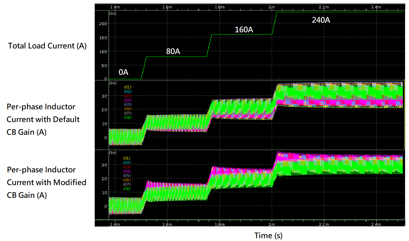
Figure 15. Current Balance Result with Symmetric PCB Layout
4.2 Practical Design Example of Type2 Common-N DCR Current Sensing (Good Layout vs. Bad Layout)
In this section, there are two practical examples of PCB layout for RT8848A with Type2 common-N DCR current sensing structure. Both of these two examples adopt the same current balance gain setup (default). The PCB trace impedance from inductor output node to GPU loading point are simulated and shown in Table 8 and Table 9. The thermal balance results of each rail are also measured and recorded in Table 8 and Table 9. The test conditions are VIN = 12V, VOUT = 0.8V, fSW = 300kHz, IOUT = 120A and TA = 25°C. The layout comparison between these two examples are shown in Figure 16 for bad layout and Figure 17 for good layout. It should be noticed that only power stage (DrMOS + Power Inductor + Output Caps.) layout are presented to reduce the layout picture size. The controller is placed away from power stage to avoid noise couple. Besides, it can be observed that the one with good layout has very symmetric output trace routing from inductor output node to GPU loading point. The current flow route of each phase is designed not to overlap another phase’s current route. This can help to prevent RPCB unbalance when there is output current on the PCB trace. On the other hand, the one with bad layout has relatively non-symmetric output trace routing from inductor output node to GPU loading point. It should be noticed that the GPU socket has been removed on EVB and the real GPU sensing point is as shown on layout. Besides, the current flow route of each phase also overlaps between each other. This makes RPCB become much more unbalance during actual loading condition. Therefore, not only current is unbalance but also the thermal balance is much worse. In a result, the RPCB layout routing has significant effect on current balance result for a common-N type DCR current sensing structure.
Table 8. PDN Design Value of Bad Layout and Thermal Balance Result
|
|
PH1
|
PH2
|
PH3
|
PH4
|
PH5
|
PH6
|
PH7
|
PH8
|
|
RPCB (mΩ)
|
0.8
|
0.79
|
0.87
|
0.97
|
1.11
|
1.26
|
1.41
|
1.58
|
|
Case Temp.
of DrMOS (°C)
|
100.2
|
86.4
|
70.3
|
57.9
|
52.8
|
46.9
|
43.7
|
42.2
|
Table 9. PDN Design Value of Good Layout and Thermal Balance Result
|
|
PH1
|
PH2
|
PH3
|
PH4
|
PH5
|
PH6
|
PH7
|
PH8
|
|
RPCB (mΩ)
|
0.55
|
0.53
|
0.56
|
0.55
|
0.55
|
0.56
|
0.53
|
0.59
|
|
Case Temp.
of DrMOS (°C)
|
64.4
|
63.4
|
61.7
|
62.1
|
62
|
61.4
|
63.9
|
63.4
|
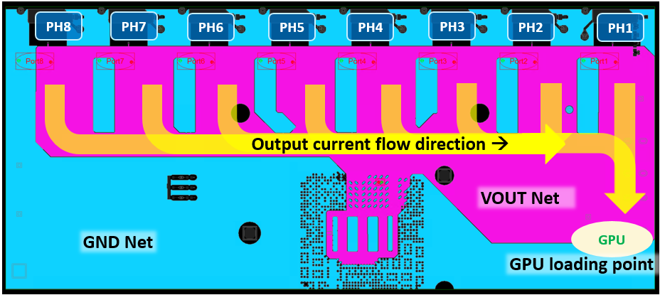
Figure 16. Power Stage Layout Diagram of RT8848A with Bad Layout
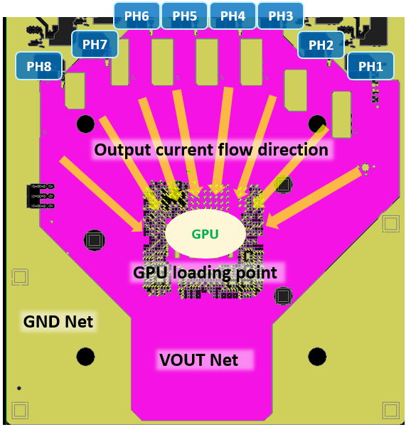
Figure 17. Power Stage Layout Diagram of RT8848A with Good Layout
4.3 Practical Design Example of Type2 & Type3 Common-N DCR Current Sensing
In this section, we will compare the current balance performance of RT8843A controller with Type2 and Type3 connection. The RT8843A is a 3 phase multi-phase synchronous Buck controller which is optimized for high performance graphic microprocessor and support Nvidia OVR3i+ specification. As shown in Figure 20(a), the RT8843A has three operating phases, and the current flows from right to left on the EVB board. The location of phase 3 is furthest away from VOUT loading point and the location of phase 1 is closest to VOUT loading point. It should be noticed that the GPU socket on EVB are disconnected, and the real GPU remoting point are as shown in Figure 20(b). Therefore, the PDN values increase gradually from phase 1 to phase 3. The experiment utilizes two different types of common-N DCR current sensing structure to compare the current balance performance. When RT8843A applies with Type2 connection as shown in Figure 18, the Rx, Cx, Rn and Cn values are designed according to equation (15) and equation (34) in previous chapters. On the other hand, when RT8843A applies with Type3 connection as shown in Figure 19, the Rx, Cx, Rm, Rn and Cn values are designed according to equation (23) and equation (34) in previous chapters. It should be noticed that the Rm value is equal to Rx for properly PCB effect cancellation and there are total 2 x 3 = 6 pcs additional Rm resistors in connection between each phase’s Cx and inductor output node. Moreover, the equivalent DCR value is reduced to 1/3 times due to Type3 connection. The test condition for both Type2 and Type3 connections are the same, VIN is set as 12V and the VOUT is 0.8V. The output load current is continuous 90A. After loading for more than 10 minutes, measuring the inductor current of each phase and case temperature of DrMOS as well. Due to RT8843A doesn’t support adjustable current balance gain, the experiments are executed with the fixed current balance gain. The test results for Type2 and Type3 are summarized in Table 10. It can be observed that the deviation of current for Type2 is around 24.7% and the deviation of current for Type3 is only 3.4%. From the test result, the Type3 performs outstanding current balance performance as compared to Type2. Although the current signal of Type3 has been degraded to 1/3 times, the RT8843A with Type3 can achieve better current balance than with Type2. It’s all credited to Type3 has good RPCB cancellation result.
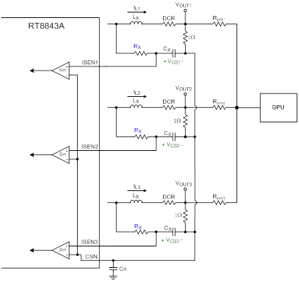
Figure 18. Simplified Application Circuit for RT8843A with Type2 DCR Current Sensing Network
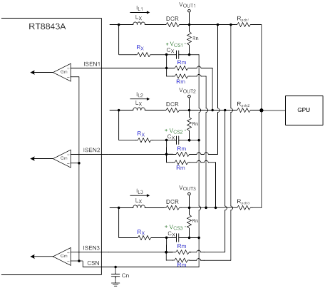
Figure 19. Simplified Application Circuit for RT8843A with Type3 DCR Current Sensing Network
Table 10. Current and Thermal Balance Result of RT8843A
|
|
Current Result (A)
|
Temperature Result (°C)
|
|
|
PH1
|
PH2
|
PH3
|
PH1
|
PH2
|
PH3
|
|
Type2
|
33.9
|
29.5
|
26.5
|
125.6
|
101.2
|
86.4
|
|
Type3
|
30.4
|
30.2
|
29.4
|
101.5
|
100.8
|
96.5
|
Figure 20. Current Flow of RT8843A (a) EVB (b) Layout
4.4 Practical Design Example of Remoting Type Common-N DCR Current Sensing
In this section, a simulation design example with remoting type of common-N DCR current sensing is presented. In this example, the RT8848A with 8 phase operation is selected to apply with remoting connection. The PDN values are assumed to be as worse as shown in Table 2. Therefore, we need to add additional Rd resistor in parallel with Cx to compensate the RPCB effect. First, due to phase 5 has the smallest RPCB value, it will be the reference value to design the other phases’ Rd value. The final design values of Rd for each phase are calculated by equation (32) and equation (33) and summarized in Table 11. As shown in Figure 21, the inductor current of each phase are almost the same at different output load current conditions. Due to the RPCB effect is cancelled by properly designing the Rd value, the correct amplitude and shape of inductor current can be sensed across Cx. Then, the RT8848A will control the PWM of each phase to balance the current according to feedback signal. However, in practical hardware implementation, the RPCB value may be different at different load condition due to different current density on PCB trace. Therefore, the current balance result may be worse than simulation result if RPCB values are not accurate. In a result, in order to achieve good current balance result and eliminate RPCB effect, the final value may be necessary to be fine tuned according to practical current measurement. The inductor current of each phase can be estimated by measuring the differential voltage across power inductor with a voltage meter (such as DMM4050). It should be noticed that the measurement result is equal to inductor average current multiplies DCR value. Moreover, due to RPCB has been considered into current sensing feedback, it would be hard to implement thermal compensation for the DCR parameters of each phase.
Table 11. Design Value of Rd for RPCB Cancellation
|
|
PH1
|
PH2
|
PH3
|
PH4
|
PH5
|
PH6
|
PH7
|
PH8
|
|
RPCB (mW)
|
1.441
|
1.401
|
1.399
|
1.406
|
0.269
|
0.378
|
0.426
|
0.472
|
|
Rd (kW)
|
1.877
|
1.943
|
1.947
|
1.935
|
Open
|
20.18
|
14.01
|
10.84
|
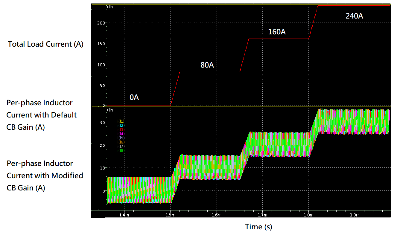
Figure 21. Current Balance Result with Remoting Cancellation
5.
Conclusion
In this application note, total of four types of DCR current sensing circuit for common-N application are introduced. We have derived the PCB effect on each type of DCR current sensing method.
For Type1 method, the PCB effect induces both DC offset and AC offset on current feedback signal. The AC offset distorts the inductor current shape and make controller unable to detect the original current signal. Besides, the DC offset makes average inductor current not proportional to DCR value. Both DC and AC offsets are severe problem to current balance control. It affects not only current balance result but also the protection functions such as OCP. Therefore, Type1 is not recommended for practical application.
For Type2 method, the hardware connection is similar to Type1, but the Rn location is different. By changing the location of Rn, the AC offset, which is generated from PCB effect, can be filtered out by Rx and Cx low pass filter. However, the inductor current signal still has DC offset. The DC offset value is related to RPCB value. The design guide and practical example are given in section 4-1. For some application with relatively symmetric layout, the RPCB effect can be compensated by adjusting the current balance gain of controller. It should be noticed that the final performance of current balance depends on the design margin of current balance gain and deviation of RPCB.
On the other hand, for Type3 method, this method requires additional resistors to be connected with Cx and each phase’s inductor output node to compensate the PCB effect. From the practical example in section 4-3, the results perform the current balance with Type3 is much better than the result with Type2. It’s credited to Type3 has good RPCB cancellation result. Nevertheless, there are two drawbacks for Type3, the first one is the additional components required to connect with each phase, and the second one is the attenuation of the DCR sense value, which may also reduce the accuracy of current signal. Generally speaking, the Type3 is more suitable for the application with less than 4 phase.
Finally, for the remoting type method, the additional Rd in parallel with Cx capacitor can effectively cancel the PCB effect. The practical example, which is shown in section 4-4, shows the current balance result of RT8848A with remoting method. Although it seems the current balance is good in simulation result, the key point is the correct value of RPCB. In order to achieve the good current balance performance, the design value of Rd may require some fine-tune processes.
In a result, the design of current sensing with DCR common-N connection is relatively hard as compared to differential type of DCR current sensing in multi-phase applications. It requires more attention and efforts on PCB layout at the beginning of system design. Although there are many methods to compensate the PCB effect in practical application, there is still a bottleneck for each method. Starting with a good PCB layout is the shortest route to achieve good current balance in common-N type applications. Besides, for some applications which require high current sensing accuracy for current reporting of each phase, the differential DCR type might be a better choice than common-N DCR type. However, if common-N DCR type is selected, the user can choose a suitable method to design their application circuit based on the comparison table as shown in Table 12.
Table 12. Comparison Table of Different Connection Types for Common-N DCR Application
|
DCR Circuit Type
|
Strength
|
Weakness
|
|
Type1
(Not recommended)
|
NA
|
1. AC and DC offset
2. Require current balance gain to compensate
|
|
Type2
|
Less components
|
1. DC offset
2. Require current balance gain to compensate
|
|
Type3
|
1. No DC offset
2. Suitable for low phase count (<4phase)
|
1. Require additional N x (N-1) pcs Rm resistors
2. Current sensing gain reduces to 1/N * DCR
3. Vcs,ofs_comp becomes crucial if 1/N * DCR is too small.
|
|
Remoting Type
|
No DC offset
|
1. Require additional Rd to compensate RPCB
2. Need to fine-tune Rd in practical application
3. Hard to measure accurate RPCB values
|
6.
Reference
[1] AN037, Comparison of DCR Current Sense Topologies.
[2] AN026, DCR Temperature Compensation
[3] RT8848A/B Datasheet
[4] RT8843A Datasheet